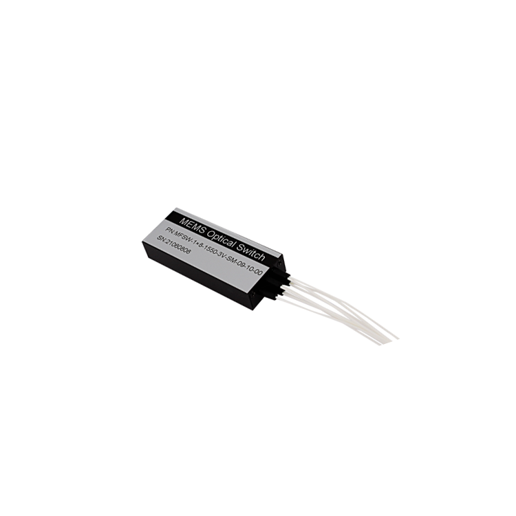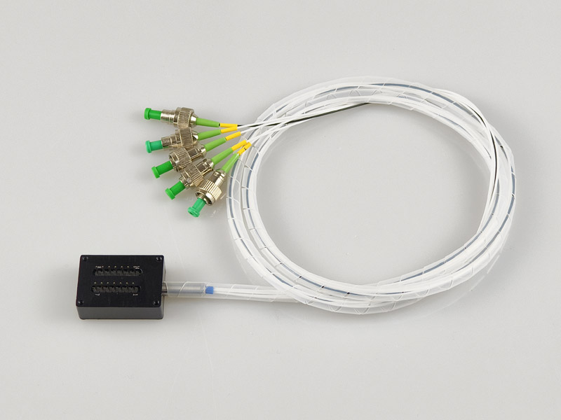
MEMS 1×N Optical Switch Module
MEMS;1x4/1x8;Optical Switch;Spot
 Huang
Email: Hqy@ybphotonics.com
Huang
Email: Hqy@ybphotonics.com
Introduction
the MEMS optical switch enables direct physical routing of optical signals without the need for opto-electrical-to-optical conversion. This provides significant advantages such as high speed, low loss, and low power consumption, making it a core component for building intelligent, flexible, and highly reliable optical communication systems.
1. Overview
A MEMS optical switch is an optical switching device based on micro-electro-mechanical systems (MEMS) technology. It utilizes the principle of light reflection and employs electrostatic actuation to control the deflection of a tiny mirror, thereby precisely controlling the transmission and switching of optical paths. As a critical fundamental component in modern optical networks, the MEMS optical switch enables direct physical routing of optical signals without the need for opto-electrical-to-optical conversion. This provides significant advantages such as high speed, low loss, and low power consumption, making it a core component for building intelligent, flexible, and highly reliable optical communication systems.
2. Features
- Modular packaging
- Fast switching speed
- Low insertion loss and high repeatability
- High reliability and stability
3.Applications
- Metropolitan Area Networks
- Data Centers
- Fiber Optic Sensing and Monitoring
- Optical Test and Measurement Systems
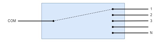
4.Optical path diagram
5. Specifications
Parameters Unit MEMS 1×N-SM(Single-mode) Operating Wavelength nm O/C/L/L+ band Test Wavelength nm 1310/1550/1625/1650 Insertion Loss dB @CWL Single-band: @CWL Dual-band: ≤0.8 (N≤8) ≤1.0 (N≤8) ≤1.0 (8<N≤16) ≤1.2 (8<N≤16) ≤1.3 (16<N≤32) ≤1.5 (16<N≤32) ≤1.5 (32<N≤64) ≤1.7 (32<N≤64) ≤2.0 (64<N≤128) ≤2.2 (64<N≤128) ≤2.2 (128<N≤256) ≤2.4 (128<N≤256) Wavelength-Dependent Loss dB ≤0.3 (N≤64) ≤0.4 (64<N≤128) ≤0.5 (128<N≤256) Polarization-Dependent Loss dB ≤0.15 Return Loss dB ≥45 Isolation dB ≥50 Repeatability dB ≤0.05 Switching Time ms ≤15 Lifespan times ≥10⁹ Maximum Optical Power mW ≤500 Operating Voltage V DC 5V±10% Operating Current mA ≤50 (N≤16) ≤250 (16<N≤64) ≤350 (64<N≤128) ≤500 (128<N≤256) Operating Temperature ℃ -20 ~ +65 Storage Temperature ℃ -40 ~ +85 Package Dimensions mm M1: 34×24×11 ±0.2 (N≤64) M2: 60×24×11 ±0.2 (N≤16) M3: 90×55×12 ±0.2 (16<N≤64) M4: 100×100×12 ±0.2 (64<N≤128) M5: 110×141×12 ±0.2 (128<N≤256)
1. All parameters were tested under room temperature conditions;
2. All parameters exclude connector insertion loss;
3. The wavelength-dependent loss test range is ±20 nm;
4. Switching time was tested using pin I/O switching;
Parameters Unit MEMS 1×N-MM(Multi-mode) Operating Wavelength ㎚ 850±30, 1310±30 Test Wavelength ㎚ 850/1310 Insertion Loss dB @CWL Single-band: @CWL Dual-band: ≤0.8 (N≤12) ≤1.0 (N≤12) ≤1.0 (12<N≤16) ≤1.2 (12<N≤16) ≤1.8 (16<N≤128) ≤2.0 (16<N≤128) Wavelength-Dependent Loss dB ≤0.3 (N≤16) ≤0.4 (16<N≤128) Polarization-Dependent Loss dB ≤0.2 Return Loss dB ≥30 Isolation dB ≥30 Repeatability dB ≤0.05 Switching Time ms ≤15 Lifespan times ≥10⁹ Maximum Optical Power mW ≤500 Operating Voltage V DC 5V±10% Operating Current mA ≤50 (N≤16) ≤250 (16<N≤64) ≤350 (64<N≤128) Operating Temperature ℃ -20 ~ +65 Storage Temperature ℃ -40 ~ +85 Package Dimensions mm M1: 34×24×11 ±0.2 (N≤16) M2: 60×24×11 ±0.2 (N≤16) M3: 90×55×12 ±0.2 (16<N≤64) M4: 100×100×12 ±0.2 (64<N≤128)
1. All parameters were tested under room temperature operating conditions;
2. All parameters exclude connector insertion loss;
3. The wavelength-dependent loss test range is ±20 nm;
4. Switching time was tested using pin I/O switching;
6.Package dimensions
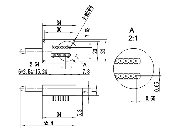
M1:34×24×11mm
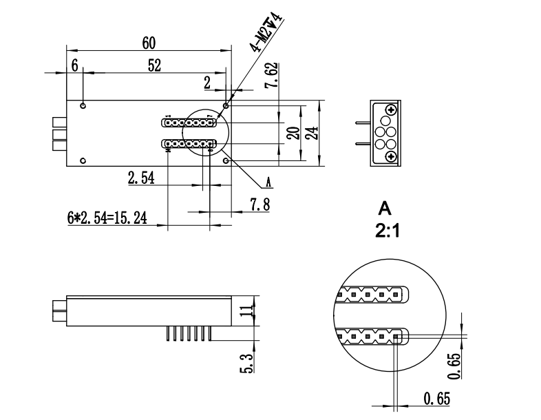
M2:60×24×11mm
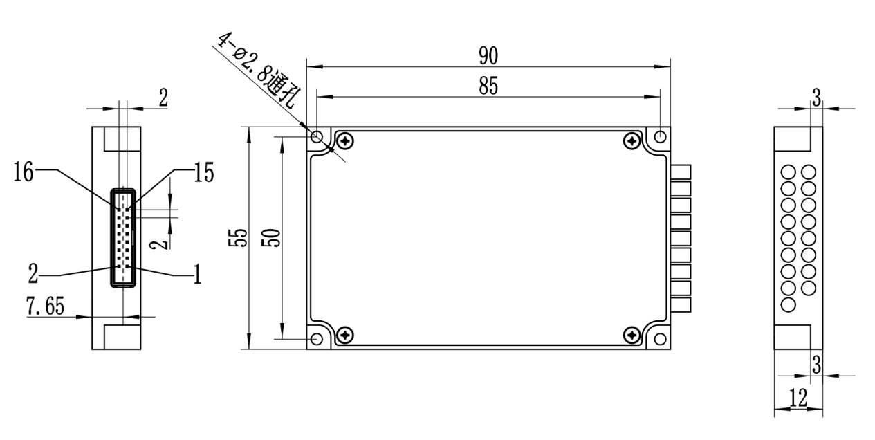
M3:90×55×12mm
TODO
M4:100×100×12mm
TODO
M5:110×141×12mm
7. Pin Definitions
Pin Number Pin Definition Signal direction, type Function Description M1/M21 M3/M4/M52 5 1 D0 Input Data Bit D0 (Lowest Bit) 3 2 D5 Input Data Bit D5 2 3 VCC Power Power Supply, DC 5V, 1.0A 4 D7 Input Data Bit D7 (Highest Bit) 5 D6 Input Data Bit D6 4 6 GND Power GND 7 D4 Input Data Bit D4 6 8 D1 Input Data Bit D1 9 9 TXD Output Serial Data Transmit (TTL 3.3V Level) 10 10 RXD Input Serial Data Receive (TTL 3.3V Level) 7 11 D2 Input Data bit D2 8 12 D3 Input Data bit D3 12 13 /BUSY Output Low level indicates readiness to reset or receive data 14 ALARM Output High level indicates an optical module operation error 3 15 /STROBE Input Data bit is executed on the falling edge 14 16 /RESET Input Reset to channel 0 on the falling edge 11 GND Power GND 13 NC Open 1 NC Open
Notes:
1. When using M1 or M2 enclosures with more than 16 channels, switching must be controlled via the serial port;
2. The electrical interfaces for M3, M4, and M5 modules use XFCN BH200R-16P;
3. The data bits D7–D0 are encoded to generate a data value; adding 1 to this value yields the channel to be switched, with the selection updated on the falling edge of the STROBE signal. For example, if the logic levels of D3, D2, D1, and D0 on an M1 module are 0, 0, 1, and 0, respectively, the encoded value is 2 in decimal. Adding 1 to this results in 3; after the STROBE signal becomes active, the module switches to channel 03.
8. Operating Instructions
1. Serial port baud rate: 9600; 8 data bits, 1 stop bit, no parity.
2. The optical switch can only execute one command at a time; you must wait for the program to return the corresponding value before entering the next command.
3. All letters in the commands must be uppercase.
4. In actual operation, use the angle bracket “<” as the start character and the angle bracket “>” as the end character.
5. OSWAA, where “AA” represents the address of the optical switch module; the default is 01.
Instruction set
Command Description Example <OSWAA_OUT_CC> Set the current channel Sending <OSW01_OUT_01> sets optical switch 1 to channel 1: AA value: 00–99 (indicates the address of the light switch module) Success response: CC value: 00–99 (indicates which channel to switch to) <OSW_OUT_OK> If the specified channel exceeds the total number of channels on the optical switch, the following response is returned: <OSW_OUT_ER> <OSWAA_OUT_?> Query the current channel of the optical switch module Sending <OSW01_OUT_?> indicates a query for optical switch channel 1: For example, a return of <OSW_OUT_03> indicates that switch 1 is channel 3.
9. Important Notes
1. Before use, clean the fiber end face of the connector with an alcohol swab. When not in use, ensure the dust cap is securely in place to prevent dust or other contaminants from contaminating or damaging the fiber end face. Damage or contamination of the fiber end face will affect the performance of the optical switch module.
2. Do not pull, bend, or twist the fiber, as this may cause damage.
3. Refer to this document for detailed pin definitions of the control interface and module installation instructions. Ensure correct wiring, and only apply power after verifying that the connections are correct.
4. Do not hot-swap the control cables while they are powered.
5. Do not look directly at the fiber end face when the optical switch module is receiving an optical signal. Laser radiation is invisible but can cause serious eye damage!
6. This device must be protected from fire and impact; avoid storing or operating it in excessively humid environments.
7. This device is a precision optical component; do not disassemble it without authorization to prevent damage.
8. When used under specified conditions, this product does not release pollutants into the atmosphere, water, or soil. The packaging does not contain hazardous waste and may be safely disposed of by the user.
9.Parts removed during product repair will be taken back by our maintenance personnel for disposal in accordance with regulations. When the product is discarded or scrapped, the user must dispose of it in accordance with environmental protection regulations.
10. Model Specifications
Ordering Information:MEMS 1×N-A-B-C-D-E-F-G
A B C Code Pattern Code wavelength Code Package dimensions S Single-mode 85 850nm M1 34×24×11mm M Multimode 13 1310nm M2 60×24×11mm 14 1490nm M3 90×55×12mm 15 1550nm M4 100×100×12mm 162 1625nm M5 110×141×12mm 165 1650nm X Other 13/15 1310/1550nm X Other D E F Code Fiber type Code Fiber diameter Code Fiber length 5 50/125 25 Φ0.25mm 5 0.5m 6 62.5/125 9 Φ0.9mm 10 1.0m 9 9/125 X Other 15 1.5m X Other X Other G Code Connector 0 无 FP FC/UPC FA FC/APC SP SC/UPC SA SC/APC LP LC/UPC LA LC/APC MP MPO X Other
11. Packing List
No. Item Name Quantity Unit Remarks 1 MEMS Optical Switch Module 1 each 2 3
the MEMS optical switch enables direct physical routing of optical signals without the need for opto-electrical-to-optical conversion. This provides significant advantages such as high speed, low loss, and low power consumption, making it a core component for building intelligent, flexible, and highly reliable optical communication systems.
1. Overview
A MEMS optical switch is an optical switching device based on micro-electro-mechanical systems (MEMS) technology. It utilizes the principle of light reflection and employs electrostatic actuation to control the deflection of a tiny mirror, thereby precisely controlling the transmission and switching of optical paths. As a critical fundamental component in modern optical networks, the MEMS optical switch enables direct physical routing of optical signals without the need for opto-electrical-to-optical conversion. This provides significant advantages such as high speed, low loss, and low power consumption, making it a core component for building intelligent, flexible, and highly reliable optical communication systems.
2. Features
- Modular packaging
- Fast switching speed
- Low insertion loss and high repeatability
- High reliability and stability
3.Applications
- Metropolitan Area Networks
- Data Centers
- Fiber Optic Sensing and Monitoring
- Optical Test and Measurement Systems
4.Optical path diagram
5. Specifications
| Parameters | Unit | MEMS 1×N-SM(Single-mode) | |
| Operating Wavelength | nm | O/C/L/L+ band | |
| Test Wavelength | nm | 1310/1550/1625/1650 | |
| Insertion Loss | dB | @CWL Single-band: | @CWL Dual-band: |
| ≤0.8 (N≤8) | ≤1.0 (N≤8) | ||
| ≤1.0 (8<N≤16) | ≤1.2 (8<N≤16) | ||
| ≤1.3 (16<N≤32) | ≤1.5 (16<N≤32) | ||
| ≤1.5 (32<N≤64) | ≤1.7 (32<N≤64) | ||
| ≤2.0 (64<N≤128) | ≤2.2 (64<N≤128) | ||
| ≤2.2 (128<N≤256) | ≤2.4 (128<N≤256) | ||
| Wavelength-Dependent Loss | dB | ≤0.3 (N≤64) | |
| ≤0.4 (64<N≤128) | |||
| ≤0.5 (128<N≤256) | |||
| Polarization-Dependent Loss | dB | ≤0.15 | |
| Return Loss | dB | ≥45 | |
| Isolation | dB | ≥50 | |
| Repeatability | dB | ≤0.05 | |
| Switching Time | ms | ≤15 | |
| Lifespan | times | ≥10⁹ | |
| Maximum Optical Power | mW | ≤500 | |
| Operating Voltage | V | DC 5V±10% | |
| Operating Current | mA | ≤50 (N≤16) | |
| ≤250 (16<N≤64) | |||
| ≤350 (64<N≤128) | |||
| ≤500 (128<N≤256) | |||
| Operating Temperature | ℃ | -20 ~ +65 | |
| Storage Temperature | ℃ | -40 ~ +85 | |
| Package Dimensions | mm | M1: 34×24×11 ±0.2 (N≤64) | |
| M2: 60×24×11 ±0.2 (N≤16) | |||
| M3: 90×55×12 ±0.2 (16<N≤64) | |||
| M4: 100×100×12 ±0.2 (64<N≤128) | |||
| M5: 110×141×12 ±0.2 (128<N≤256) | |||
1. All parameters were tested under room temperature conditions;
2. All parameters exclude connector insertion loss;
3. The wavelength-dependent loss test range is ±20 nm;
4. Switching time was tested using pin I/O switching;
| Parameters | Unit | MEMS 1×N-MM(Multi-mode) | |
| Operating Wavelength | ㎚ | 850±30, 1310±30 | |
| Test Wavelength | ㎚ | 850/1310 | |
| Insertion Loss | dB | @CWL Single-band: | @CWL Dual-band: |
| ≤0.8 (N≤12) | ≤1.0 (N≤12) | ||
| ≤1.0 (12<N≤16) | ≤1.2 (12<N≤16) | ||
| ≤1.8 (16<N≤128) | ≤2.0 (16<N≤128) | ||
| Wavelength-Dependent Loss | dB | ≤0.3 (N≤16) | |
| ≤0.4 (16<N≤128) | |||
| Polarization-Dependent Loss | dB | ≤0.2 | |
| Return Loss | dB | ≥30 | |
| Isolation | dB | ≥30 | |
| Repeatability | dB | ≤0.05 | |
| Switching Time | ms | ≤15 | |
| Lifespan | times | ≥10⁹ | |
| Maximum Optical Power | mW | ≤500 | |
| Operating Voltage | V | DC 5V±10% | |
| Operating Current | mA | ≤50 (N≤16) | |
| ≤250 (16<N≤64) | |||
| ≤350 (64<N≤128) | |||
| Operating Temperature | ℃ | -20 ~ +65 | |
| Storage Temperature | ℃ | -40 ~ +85 | |
| Package Dimensions | mm | M1: 34×24×11 ±0.2 (N≤16) | |
| M2: 60×24×11 ±0.2 (N≤16) | |||
| M3: 90×55×12 ±0.2 (16<N≤64) | |||
| M4: 100×100×12 ±0.2 (64<N≤128) | |||
1. All parameters were tested under room temperature operating conditions;
2. All parameters exclude connector insertion loss;
3. The wavelength-dependent loss test range is ±20 nm;
4. Switching time was tested using pin I/O switching;
6.Package dimensions
M1:34×24×11mm
M2:60×24×11mm
M3:90×55×12mm
TODO
M4:100×100×12mm
TODO
M5:110×141×12mm
7. Pin Definitions
| Pin Number | Pin Definition | Signal direction, type | Function Description | |
| M1/M21 | M3/M4/M52 | |||
| 5 | 1 | D0 | Input | Data Bit D0 (Lowest Bit) 3 |
| 2 | D5 | Input | Data Bit D5 | |
| 2 | 3 | VCC | Power | Power Supply, DC 5V, 1.0A |
| 4 | D7 | Input | Data Bit D7 (Highest Bit) | |
| 5 | D6 | Input | Data Bit D6 | |
| 4 | 6 | GND | Power | GND |
| 7 | D4 | Input | Data Bit D4 | |
| 6 | 8 | D1 | Input | Data Bit D1 |
| 9 | 9 | TXD | Output | Serial Data Transmit (TTL 3.3V Level) |
| 10 | 10 | RXD | Input | Serial Data Receive (TTL 3.3V Level) |
| 7 | 11 | D2 | Input | Data bit D2 |
| 8 | 12 | D3 | Input | Data bit D3 |
| 12 | 13 | /BUSY | Output | Low level indicates readiness to reset or receive data |
| 14 | ALARM | Output | High level indicates an optical module operation error | |
| 3 | 15 | /STROBE | Input | Data bit is executed on the falling edge |
| 14 | 16 | /RESET | Input | Reset to channel 0 on the falling edge |
| 11 | GND | Power | GND | |
| 13 | NC | Open | ||
| 1 | NC | Open | ||
Notes:
1. When using M1 or M2 enclosures with more than 16 channels, switching must be controlled via the serial port;
2. The electrical interfaces for M3, M4, and M5 modules use XFCN BH200R-16P;
3. The data bits D7–D0 are encoded to generate a data value; adding 1 to this value yields the channel to be switched, with the selection updated on the falling edge of the STROBE signal. For example, if the logic levels of D3, D2, D1, and D0 on an M1 module are 0, 0, 1, and 0, respectively, the encoded value is 2 in decimal. Adding 1 to this results in 3; after the STROBE signal becomes active, the module switches to channel 03.
8. Operating Instructions
1. Serial port baud rate: 9600; 8 data bits, 1 stop bit, no parity.
2. The optical switch can only execute one command at a time; you must wait for the program to return the corresponding value before entering the next command.
3. All letters in the commands must be uppercase.
4. In actual operation, use the angle bracket “<” as the start character and the angle bracket “>” as the end character.
5. OSWAA, where “AA” represents the address of the optical switch module; the default is 01.
Instruction set
| Command | Description | Example |
| <OSWAA_OUT_CC> | Set the current channel | Sending <OSW01_OUT_01> sets optical switch 1 to channel 1: |
| AA value: 00–99 (indicates the address of the light switch module) | Success response: | |
| CC value: 00–99 (indicates which channel to switch to) | <OSW_OUT_OK> | |
| If the specified channel exceeds the total number of channels on the optical switch, the following response is returned: | ||
| <OSW_OUT_ER> | ||
| <OSWAA_OUT_?> | Query the current channel of the optical switch module | Sending <OSW01_OUT_?> indicates a query for optical switch channel 1: |
| For example, a return of <OSW_OUT_03> indicates that switch 1 is channel 3. |
9. Important Notes
1. Before use, clean the fiber end face of the connector with an alcohol swab. When not in use, ensure the dust cap is securely in place to prevent dust or other contaminants from contaminating or damaging the fiber end face. Damage or contamination of the fiber end face will affect the performance of the optical switch module.
2. Do not pull, bend, or twist the fiber, as this may cause damage.
3. Refer to this document for detailed pin definitions of the control interface and module installation instructions. Ensure correct wiring, and only apply power after verifying that the connections are correct.
4. Do not hot-swap the control cables while they are powered.
5. Do not look directly at the fiber end face when the optical switch module is receiving an optical signal. Laser radiation is invisible but can cause serious eye damage!
6. This device must be protected from fire and impact; avoid storing or operating it in excessively humid environments.
7. This device is a precision optical component; do not disassemble it without authorization to prevent damage.
8. When used under specified conditions, this product does not release pollutants into the atmosphere, water, or soil. The packaging does not contain hazardous waste and may be safely disposed of by the user.
9.Parts removed during product repair will be taken back by our maintenance personnel for disposal in accordance with regulations. When the product is discarded or scrapped, the user must dispose of it in accordance with environmental protection regulations.
10. Model Specifications
Ordering Information:MEMS 1×N-A-B-C-D-E-F-G
| A | B | C | |||||
| Code | Pattern | Code | wavelength | Code | Package dimensions | ||
| S | Single-mode | 85 | 850nm | M1 | 34×24×11mm | ||
| M | Multimode | 13 | 1310nm | M2 | 60×24×11mm | ||
| 14 | 1490nm | M3 | 90×55×12mm | ||||
| 15 | 1550nm | M4 | 100×100×12mm | ||||
| 162 | 1625nm | M5 | 110×141×12mm | ||||
| 165 | 1650nm | X | Other | ||||
| 13/15 | 1310/1550nm | ||||||
| X | Other | ||||||
| D | E | F | |||||
| Code | Fiber type | Code | Fiber diameter | Code | Fiber length | ||
| 5 | 50/125 | 25 | Φ0.25mm | 5 | 0.5m | ||
| 6 | 62.5/125 | 9 | Φ0.9mm | 10 | 1.0m | ||
| 9 | 9/125 | X | Other | 15 | 1.5m | ||
| X | Other | X | Other | ||||
| G | |||||||
| Code | Connector | ||||||
| 0 | 无 | ||||||
| FP | FC/UPC | ||||||
| FA | FC/APC | ||||||
| SP | SC/UPC | ||||||
| SA | SC/APC | ||||||
| LP | LC/UPC | ||||||
| LA | LC/APC | ||||||
| MP | MPO | ||||||
| X | Other | ||||||
11. Packing List
| No. | Item Name | Quantity | Unit | Remarks |
|---|---|---|---|---|
| 1 | MEMS Optical Switch Module | 1 | each | |
| 2 | ||||
| 3 |