<
>
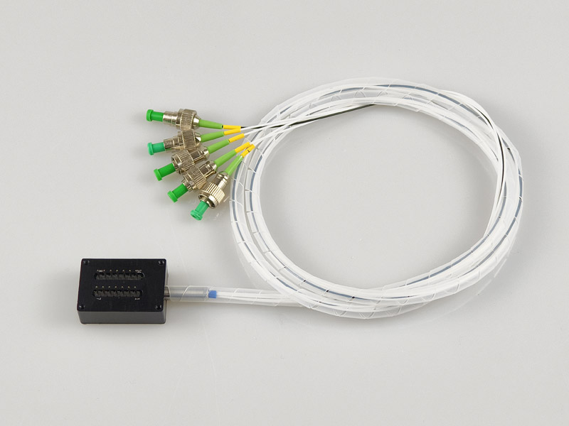
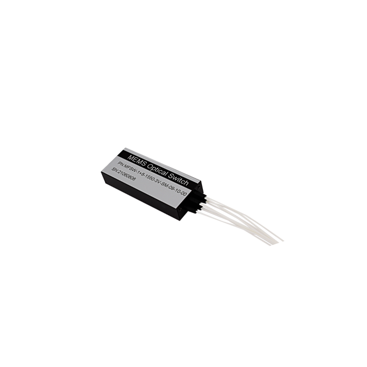
MEMS 1×N Optical Switch Module
MEMS 1×N Optical Switch Module
Model:MEMS 1×N-A-B-C-D-E-F-G
Contact: Huang
Email: Hqy@ybphotonics.com
Huang
Email: Hqy@ybphotonics.com
Huang
Email: Hqy@ybphotonics.com
Introduction
MEMS 1×N optical switch module can be used in fiber optic sensing and monitoring, instrumentation, metro network and other applications.
Product Characteristics
- modular package
- Fast switching speed
- Low insertion loss, good repeatability
- High reliability and stability
Applications
- metropolitan area network
- data center
- Fiber Optic Sensing and Monitoring
- Instruments and meters
Compliance with standards
- Telcordia GR-1221
- Telcordia GR-1073
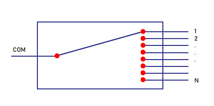
Optical pathway diagram
Specifications (single mode)
parameters Unit MEMS 1×N-SM Working wavelength nm O/C/L/L+ band Test wavelength nm 1310/1550/1625/1650 insertion loss dB @CWL Single-band≤0.8 (N≤8)≤1.0 (8<N≤16)≤1.3 (16<N≤32)≤1.5 (32<N≤64)≤2.0 (64<N≤144)≤2.2 (144<N≤256) @CWL Dual-band≤1.0 (N≤8)≤1.2 (8<N≤16)≤1.5 (16<N≤32)≤1.7 (32<N≤64)≤2.2 (64<N≤144)≤2.4 (144<N≤256) Wavelength dependent loss dB ≤0.3 (N≤64)≤0.4 (64<N≤144)≤0.5 (144<N≤256) Polarization-related losses dB ≤0.15 return loss dB ≥45 Crosstalk dB ≥50 repeatable dB ≤±0.05 switching time ms ≤15 longevity times ≥109 Maximum optical power mW ≤500 operating voltage V DC 5V±10% Operating Current mA ≤50 (N≤16)≤250 (16<N≤64)≤350 (64<N≤144)≤500 (144<N≤256) operating temperature °C -20 ~ +85 Storage temperature °C -40 ~ +85 Package Size mm M1: 34×24×11 ±0.2 (N≤64, Bare Fiber)M2: 60×24×11 ±0.2 (N≤16, Loose Tube)M3: 90×55×12 ±0.2 (16<N≤64, Loose Tube)M4: 100×100×12 ±0.2 (64<N≤144, Loose Tube)M5: 110×141×12 ±0.2 (144<N≤256, Loose Tube) 1. All parameters are tested under room temperature working environment; 2. All parameters do not include the connector insertion loss; 3. The wavelength dependent loss test range is ±20nm.
Specifications (multimode)
parameters Unit MEMS 1×N-MM Working wavelength nm 850±30, 1310±30 Test wavelength nm 850/1310 insertion loss dB @CWL Single-band≤0.8 (N≤12)≤1.0 (12<N≤16)≤1.8 (16<N≤128) @CWL Dual-band≤1.0 (N≤12)≤1.2 (12<N≤16)≤2.0 (16<N≤128) Wavelength dependent loss dB ≤0.3 (N≤16)≤0.4 (16<N≤128) Polarization-related losses dB ≤0.2 return loss dB ≥30 Crosstalk dB ≥30 repeatable dB ≤±0.05 switching time ms ≤15 longevity times ≥109 Maximum optical power mW ≤500 operating voltage V DC 5V±10% Operating Current mA ≤50 (N≤16)≤250 (16<N≤64)≤350 (64<N≤128) operating temperature °C -20 ~ +85 Storage temperature °C -40 ~ +85 Package Size mm M1: 34×24×11 ±0.2 (N≤16, Bare Fiber)M2: 60×24×11 ±0.2 (N≤16, Loose Tube)M3: 90×55×12 ±0.2 (16<N≤64, Loose Tube)M4: 100×100×12 ±0.2 (64<N≤128, Loose Tube) 1. All parameters are tested under room temperature working environment; 2. All parameters do not include the connector insertion loss; 3. The wavelength dependent loss test range is ±20nm.
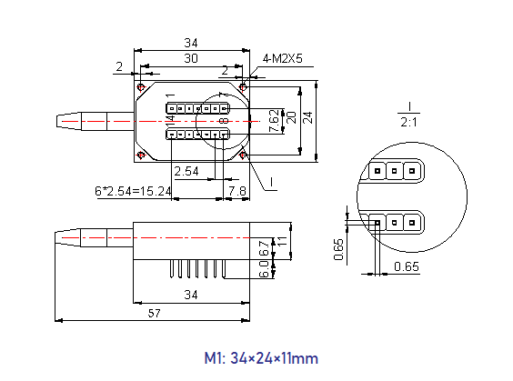
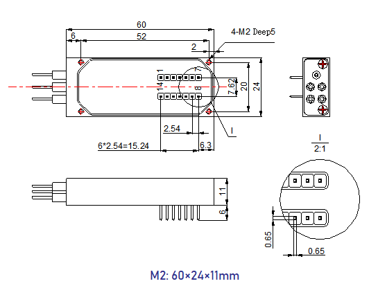
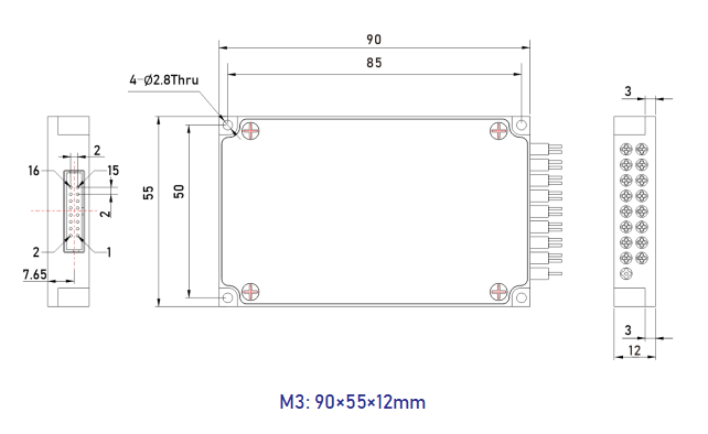
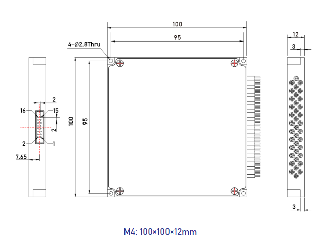
Package Size
Pin Definitions
Pin Number Pin Definitions
Signal direction, type
Functional Description
M1/M2 M3/M4/M5 5 1 D0 Input Data bit D0 (low) 2 D5 Input Data bit D5 2 3 VCC Power Operating power supply, DC 5V, 1.0A 4 D7 Input Data bit D7 (high) 5 D6 Input Data Bit D6 4 6 GND Power GND 7 D4 Input Data bit D4 6 8 D1 Input Data bit D1 9 9 TXD Output Serial data sender (TTL level serial port) 10 10 RXD Input Serial data receiver (TTL level serial port) 7 11 D2 Input Data bit D2 8 12 D3 Input Data Bit D3 12 13 /BUSY Output Low ready to reset or receive data. 14 /ALARM Output A high level indicates an optical module operation error. 3 15 /STROBE Input The falling edge executes the data bits. 14 16 /RESET Input Reset low to channel 0. 11 GND Power GND 13 MODE Low level data bit control toggle, high level UART control toggle 1 NC vacant
MEMS 1×N optical switch module can be used in fiber optic sensing and monitoring, instrumentation, metro network and other applications.
Product Characteristics
- modular package
- Fast switching speed
- Low insertion loss, good repeatability
- High reliability and stability
Applications
- metropolitan area network
- data center
- Fiber Optic Sensing and Monitoring
- Instruments and meters
Compliance with standards
- Telcordia GR-1221
- Telcordia GR-1073
Optical pathway diagram
Specifications (single mode)
| parameters | Unit | MEMS 1×N-SM | |
|---|---|---|---|
| Working wavelength | nm | O/C/L/L+ band | |
| Test wavelength | nm | 1310/1550/1625/1650 | |
| insertion loss | dB | @CWL Single-band≤0.8 (N≤8)≤1.0 (8<N≤16)≤1.3 (16<N≤32)≤1.5 (32<N≤64)≤2.0 (64<N≤144)≤2.2 (144<N≤256) | @CWL Dual-band≤1.0 (N≤8)≤1.2 (8<N≤16)≤1.5 (16<N≤32)≤1.7 (32<N≤64)≤2.2 (64<N≤144)≤2.4 (144<N≤256) |
| Wavelength dependent loss | dB | ≤0.3 (N≤64)≤0.4 (64<N≤144)≤0.5 (144<N≤256) | |
| Polarization-related losses | dB | ≤0.15 | |
| return loss | dB | ≥45 | |
| Crosstalk | dB | ≥50 | |
| repeatable | dB | ≤±0.05 | |
| switching time | ms | ≤15 | |
| longevity | times | ≥109 | |
| Maximum optical power | mW | ≤500 | |
| operating voltage | V | DC 5V±10% | |
| Operating Current | mA | ≤50 (N≤16)≤250 (16<N≤64)≤350 (64<N≤144)≤500 (144<N≤256) | |
| operating temperature | °C | -20 ~ +85 | |
| Storage temperature | °C | -40 ~ +85 | |
| Package Size | mm | M1: 34×24×11 ±0.2 (N≤64, Bare Fiber)M2: 60×24×11 ±0.2 (N≤16, Loose Tube)M3: 90×55×12 ±0.2 (16<N≤64, Loose Tube)M4: 100×100×12 ±0.2 (64<N≤144, Loose Tube)M5: 110×141×12 ±0.2 (144<N≤256, Loose Tube) | |
| 1. All parameters are tested under room temperature working environment; 2. All parameters do not include the connector insertion loss; 3. The wavelength dependent loss test range is ±20nm. | |||
Specifications (multimode)
| parameters | Unit | MEMS 1×N-MM | |
|---|---|---|---|
| Working wavelength | nm | 850±30, 1310±30 | |
| Test wavelength | nm | 850/1310 | |
| insertion loss | dB | @CWL Single-band≤0.8 (N≤12)≤1.0 (12<N≤16)≤1.8 (16<N≤128) | @CWL Dual-band≤1.0 (N≤12)≤1.2 (12<N≤16)≤2.0 (16<N≤128) |
| Wavelength dependent loss | dB | ≤0.3 (N≤16)≤0.4 (16<N≤128) | |
| Polarization-related losses | dB | ≤0.2 | |
| return loss | dB | ≥30 | |
| Crosstalk | dB | ≥30 | |
| repeatable | dB | ≤±0.05 | |
| switching time | ms | ≤15 | |
| longevity | times | ≥109 | |
| Maximum optical power | mW | ≤500 | |
| operating voltage | V | DC 5V±10% | |
| Operating Current | mA | ≤50 (N≤16)≤250 (16<N≤64)≤350 (64<N≤128) | |
| operating temperature | °C | -20 ~ +85 | |
| Storage temperature | °C | -40 ~ +85 | |
| Package Size | mm | M1: 34×24×11 ±0.2 (N≤16, Bare Fiber)M2: 60×24×11 ±0.2 (N≤16, Loose Tube)M3: 90×55×12 ±0.2 (16<N≤64, Loose Tube)M4: 100×100×12 ±0.2 (64<N≤128, Loose Tube) | |
| 1. All parameters are tested under room temperature working environment; 2. All parameters do not include the connector insertion loss; 3. The wavelength dependent loss test range is ±20nm. | |||
Package Size
Pin Definitions
| Pin Number | Pin Definitions | Signal direction, type | Functional Description | |
|---|---|---|---|---|
| M1/M2 | M3/M4/M5 | |||
| 5 | 1 | D0 | Input | Data bit D0 (low) |
| 2 | D5 | Input | Data bit D5 | |
| 2 | 3 | VCC | Power | Operating power supply, DC 5V, 1.0A |
| 4 | D7 | Input | Data bit D7 (high) | |
| 5 | D6 | Input | Data Bit D6 | |
| 4 | 6 | GND | Power | GND |
| 7 | D4 | Input | Data bit D4 | |
| 6 | 8 | D1 | Input | Data bit D1 |
| 9 | 9 | TXD | Output | Serial data sender (TTL level serial port) |
| 10 | 10 | RXD | Input | Serial data receiver (TTL level serial port) |
| 7 | 11 | D2 | Input | Data bit D2 |
| 8 | 12 | D3 | Input | Data Bit D3 |
| 12 | 13 | /BUSY | Output | Low ready to reset or receive data. |
| 14 | /ALARM | Output | A high level indicates an optical module operation error. | |
| 3 | 15 | /STROBE | Input | The falling edge executes the data bits. |
| 14 | 16 | /RESET | Input | Reset low to channel 0. |
| 11 | GND | Power | GND | |
| 13 | MODE | Low level data bit control toggle, high level UART control toggle | ||
| 1 | NC | vacant |
Product Inquiry
Leading manufacturer of photodetector modules and fiber optic sensing system modules