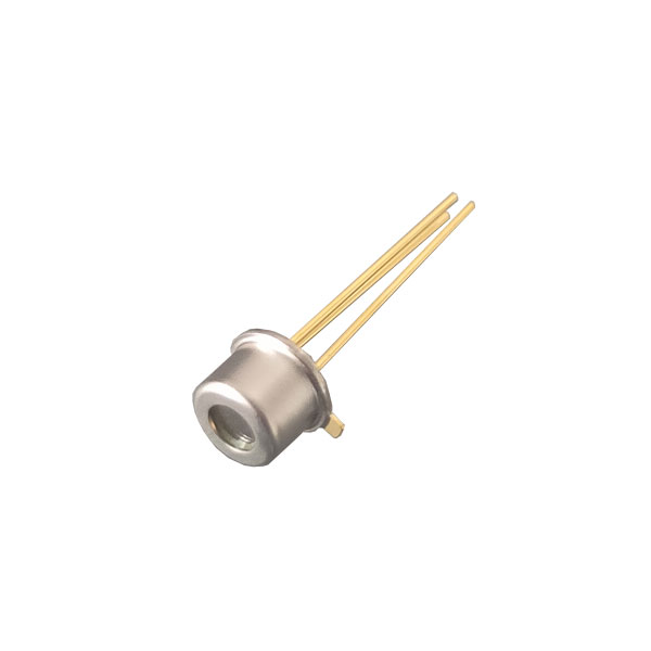
InGaAs Avalanche Photodiode 2000um APD Chip
InGaAs;photodiode;2000μm;2mm;TO-39;APD chip;avalanche Photodiode
 Huang
Email: Hqy@ybphotonics.com
Huang
Email: Hqy@ybphotonics.com
Introduction
ingaas avalanche photodiode, Φ 2000μm, used for Distance measurement, Spatial light transmission, available in bare die, TO-39
Features
- High responsivity
- Low capacitance
- Low dark current
Product Specifications
Absolute Maximum Ratings
Parameter Symbol Min. Type. Max. Unit Storage Temperature Tstg -40 125 ℃ Operating Temperature Tc -40 — 85 ℃ Reverse Current IR — — 10 mA Forward Current IF — — 10 mA Soldering Temperature /Time Tsld/t 260/10 ℃/s
Electro-Optical Characteristics (@ Tc=22±3℃)
Parameter Test Condition Min. Typ. Max. Unit Responsivity1 λ=1310nm 0.9 0.98 —— A/W Responsivity2 λ=1550nm 0.95 1.1 —— A/W Dark Current V=-1V —— 0.6 5 nA V=-5V —— 2 20 nA Breakdown Voltage I=-10µA 40 —— —— V Capacitance V=-2V,f=1MHz —— 220 250 pF V=-5V,f=1MHz —— 170 200 pF Forward Voltage I=1mA —— 0.39 0.7 V
Dimensions
As shown in Figure 1
Parameter Min. Typ. Max. Unit Notes Die Width 2190 2200 2210 µm Die Length 2190 2200 2210 µm Detection Window —— 2000 —— µm Thickness 190 200 210 µm Bonding Pad Diameter —— 150 —— µm For p-pad
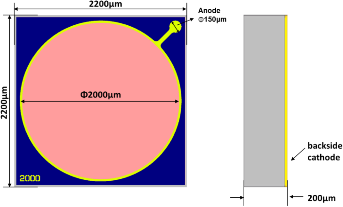
Figure 1
Attention: Handle with care, InP is a brittle material. The device can be permanently damaged when exposed to ESD.Specifications are subject to change without notice.
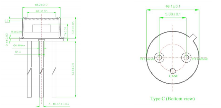
Outline Diagram (in mm):
Ordering Information:
GY TG _C FW _0 MTP F
TO Type:TO39 Pin Type:C Cap Type:Flat Windows Product Type:PIN Chip Type:GYMPD2000V1 SupplierCode
Product Compliance Information:
RoHS Compliance
This part is compliant with 2011/65/EU and 2015/863 RoHS directive (Restrictions on the Use of Certain Hazardous Substances in Electrical and Electronic Equipment).
Precaution:
(1) The modules should be handled in the same manner as ordinary semiconductor device to prevent the electro-static damages. The modules should be packaged with ESD proof material for safety keeping and carrying. The workbench, the soldering iron, and the human body should be grounded during the assembly of the modules.
(2) Please pay special attention to the atmosphere condition because the dew on the modules may cause electrical damages.
ingaas avalanche photodiode, Φ 2000μm, used for Distance measurement, Spatial light transmission, available in bare die, TO-39
Features
- High responsivity
- Low capacitance
- Low dark current
Product Specifications
Absolute Maximum Ratings
| Parameter | Symbol | Min. | Type. | Max. | Unit |
|---|---|---|---|---|---|
| Storage Temperature | Tstg | -40 | 125 | ℃ | |
| Operating Temperature | Tc | -40 | — | 85 | ℃ |
| Reverse Current | IR | — | — | 10 | mA |
| Forward Current | IF | — | — | 10 | mA |
| Soldering Temperature /Time | Tsld/t | 260/10 | ℃/s |
Electro-Optical Characteristics (@ Tc=22±3℃)
| Parameter | Test Condition | Min. | Typ. | Max. | Unit |
|---|---|---|---|---|---|
| Responsivity1 | λ=1310nm | 0.9 | 0.98 | —— | A/W |
| Responsivity2 | λ=1550nm | 0.95 | 1.1 | —— | A/W |
| Dark Current | V=-1V | —— | 0.6 | 5 | nA |
| V=-5V | —— | 2 | 20 | nA | |
| Breakdown Voltage | I=-10µA | 40 | —— | —— | V |
| Capacitance | V=-2V,f=1MHz | —— | 220 | 250 | pF |
| V=-5V,f=1MHz | —— | 170 | 200 | pF | |
| Forward Voltage | I=1mA | —— | 0.39 | 0.7 | V |
Dimensions
As shown in Figure 1
| Parameter | Min. | Typ. | Max. | Unit | Notes |
|---|---|---|---|---|---|
| Die Width | 2190 | 2200 | 2210 | µm | |
| Die Length | 2190 | 2200 | 2210 | µm | |
| Detection Window | —— | 2000 | —— | µm | |
| Thickness | 190 | 200 | 210 | µm | |
| Bonding Pad Diameter | —— | 150 | —— | µm | For p-pad |
Figure 1
Attention: Handle with care, InP is a brittle material. The device can be permanently damaged when exposed to ESD.Specifications are subject to change without notice.
Outline Diagram (in mm):
| GY | TG | _C | FW | _0 | MTP | F |
|---|---|---|---|---|---|---|
| TO Type:TO39 | Pin Type:C | Cap Type:Flat Windows | Product Type:PIN | Chip Type:GYMPD2000V1 | SupplierCode |
Product Compliance Information:
RoHS Compliance
This part is compliant with 2011/65/EU and 2015/863 RoHS directive (Restrictions on the Use of Certain Hazardous Substances in Electrical and Electronic Equipment).
Precaution:
(1) The modules should be handled in the same manner as ordinary semiconductor device to prevent the electro-static damages. The modules should be packaged with ESD proof material for safety keeping and carrying. The workbench, the soldering iron, and the human body should be grounded during the assembly of the modules.
(2) Please pay special attention to the atmosphere condition because the dew on the modules may cause electrical damages.
